Scope of the school
MINATO summer school is a summer school on Micro and Nano-fabrication tools for innovating applied electronics and fundamental research. The objective for each student will be to acquire new scientific skills and knowledge, both theoretical and practical, in the field of nanoscience and nanotechnology.
Scientific positioning
The Summer School aims at introducing micro&nano fabrication techniques, with a hands-on interdisciplinary approach that alternates basic lectures and experimental activities. The core of the summer school will be mainly on the uses of these technologies, starting from virgin Silicon wafer to building up and exploiting a fully functional device. Over two or four weeks, after a series of introduction lectures, each student will take in charge the micro&nano fabrication and characterization of its own device using clean room facilities (MOS electronics, solar cell, micro-super condensator, gas sensor,
2D material-based devices, …).
Keywords: Clean room, Nanoscale Science and Engineering Microelectronics, Nanotechnology, Nanochemistry, Nanophysics, Energy harvesting and storage, Semiconductor and 2D Materials
Pedagogic Objectives
The objective for each student will be to acquire new scientific skills and knowledge, both theoretical and practical, in the field of nanoscience and nanotechnology.
By the end of the summer school, students should have understood and be able to explain (main concepts):
1/ Theoretical and practical knowledge of manufacturing processes for nanostructures and integrated components in Silicon technology
2/ Electronic and optical properties of nanostructures and simple electronic components (diode, transistor, chemical sensor, photo-voltaic cell, micro-supercapacitor, semiconductor and 2D material, etc.). Quantum technology.
The student should be able to :
– Design and implement manufacturing processes for nanostructures/nanodevice or integrated components in Si technology, with defined functionality in terms of electronic, optical, physical or chemical properties.
– Produce nanostructures by physical or chemical means (vacuum deposition, vapor deposition, Si doping).
– Use lithography techniques.
– Understand the wet or dry etching techniques.
– Carry out morphological characterizations of nanostructures.
– Test, interpret and analyze electrical and optical properties of nanostructures or integrated component.
– Control quality at every stage of a complex manufacturing process.
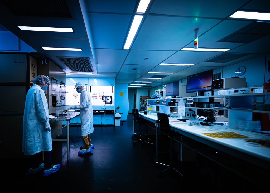
– Work in a complex cleanroom environment, applying best practices, following a quality approach and complying with safety rules, particularly with regard to chemical risks.
– Communicating in French: mastering the basics of oral and written French. Objective level A0-A1 / Beginner
School organisation
The total number of students is limited to 24. The schedule of the school is :
a. Introductory Micromodule
Enrolled students will follow an online micromodule, which aims to provide a basic foundation of concepts and knowledge on the topics that will be covered during the summer school (course 5h). Each student will have to produce a small video presentation on a specified topic on micro- and nano-technology.
b. Introduction Lectures
Students will take lectures on the state of the art in nanotechnology, methods for the elaboration of micro-nanomaterials, process design for the manufacture of nanostructures and integrated components, characterizations and quality control at the various stages, and property measurements.
- Introduction to micro and nano-technologies (2h)
- Basics and physics of semi-conductors (4h)
- Physical elaboration (thin film deposition techniques) (1h30)
- Chemical elaboration (nanoparticle elaboration using chemical methods) (1h30)
- Lithography techniques (2h)
- Chemical process (cleaning, wet etching, …) (2h)
- Simulation and design of technology, components and integrated circuits (3h)
- Optic* (2h)
- Basics of quantum mechanics* (*4 week school) (4h)
c. Labwork
Students will follow one or two thematic Labwork of their choice. For each thematic, they will be divided into small groups (4 to 6 students) and follow lab work in a clean room (2 x 25h of lab work). In order to facilitate understanding and result interpretation, they are supplemented by remediation time (2 x 5 hours tutorials) and specific lecture courses (2 x 1 hour lectures), and laboratory visits.
- Microelectronics – MOS (metal oxide semiconductor) technology (elementary components, diode, transistor, integrated circuits)
- Energy : integrated energy harvesting (solar cell) and storage (micro-supercondensator) technologies
- Nano – Chemistry : chemical sensors based on metal oxide semi-conductors nano-objects
- Nano – Physics : remarkable properties of devices integrating 2D materials (graphene, …)
- Quantum technologies : ultrasensitive sensors and quantum cryptography* (*only for 4 weeks program)
Previsional program (2 and 4 weeks duration)

Direction of the school
Prof. Marc Respaud
Organising commitee
Prof. Marc Respaud
Dr. Reasmey Tan
Dr. Jean-Baptiste Lincelles
Dr. Justine Harmel
Dr. Walter Escoffier
Prof. Xavier Marie